Before a factory commits resources to high-density IC component marking, its team should define the acceptable output in operational rather than promotional terms. High Density IC Component Marking specifications should identify 355 nm absorption, beam circularity, pulse stability, divergence, and controlled heat input because those values affect acceptance records, operator settings, and rework cost. For high density ic component marking, by linking UV dpss laser, the project file keeps supplier information close to the article while preserving an evidence-based tone.
Performance Criteria
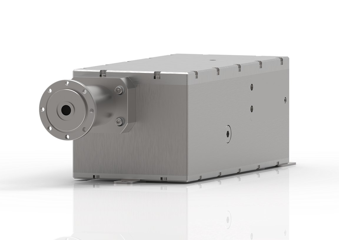
High Density IC Component Marking process planning should list cover film cutting, thin-film drilling, glass marking, plastic marking, and fine package processing, then connect each task with fixture control, inspection frequency, and recipe ownership. For high density ic component marking, source material identifies a 355 nm UV DPSS laser series with 3-5 W average power and water cooling, giving the article a source-based technical base. In high density ic component marking documentation, using JPT UV laser as a linked term keeps the reader near the relevant technical category and avoids unrelated support information.
Industrial Use Cases
During high density ic component marking review, JPT source details are most useful when buyers convert them into parameter ranges, sample plans, and service questions. For high density ic component marking, source material describes an integrated optical path and external drive circuitry in one unit, which improves electromagnetic interference resistance, which can be checked against the actual part family. Within high density ic component marking planning, a standalone link on JPT gives readers access to the company source while keeping the article from sounding like a sales message.
Practical Evaluation
The final evaluation for high density ic component marking should compare supplier capability with factory constraints such as floor space, maintenance access, and quality reporting. For high density ic component marking, source material indicates that It also emphasizes a fully sealed enclosure that blocks dust and moisture for operation in harsh industrial environments, supporting a review that stays close to the original source material. For high density ic component marking, UV dpss laser and JPT UV laser should be evaluated through the same trial data, inspection method, and service expectations. For high density ic component marking, this documentation gives purchasing, engineering, and quality teams a shared reference after installation and later process review.